


New Bricktronics Updates!
Today at the Bay Area Maker Faire, we are announcing a couple of cool new projects we’ve been working on with the Bricktronics Kits.
![]()
1. Bricktronics Megashield – Build robots and contraptions! Experiment with mechatronics using Arduino and LEGO Mindstorms NXT! Our latest kit, the Bricktronics Megashield, to connect up to and to an Arduino Mega. Works with the standard LEGO NXT motors and the touch, ultrasonic, and color sensors. Uses the same easy-to-use software interface as the original Bricktronics Shield, but supports more motors and supports all types of sensors on all ports.
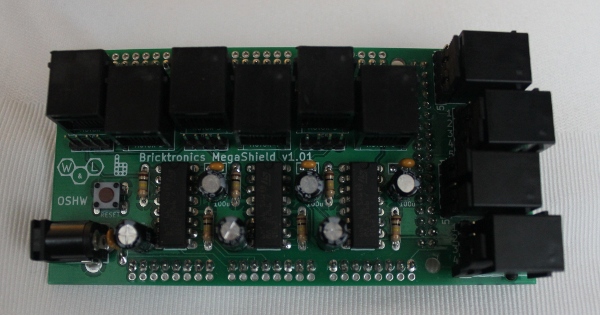
The Megashield is available for purchase at the Maker Faire this weekend, and is now available for purchase from the Wayne and Layne store!

2. Project codename “Trifrost” – We created a small python web framework for connecting local serial devices (such as an Arduino) to Linux computers (such as the RaspberryPi and the BeagleBone) to get real-time web dashboards and interactivity. This is still a work in progress, and we have tons of ideas for extending and enhancing it, so stay tuned.

3. Bricktronics + RaspberryPi = Awesome! – The Raspberry Pi and other low-cost embedded Linux single-board computers are all the rage these days! We combined an Arduino with Shields, and connected them to a RasberryPi, to create a high-power interactive robotics platform. Using a WiFi adapter and a tablet computer, you can use the touchscreen to wirelessly interact with the motors and sensors.
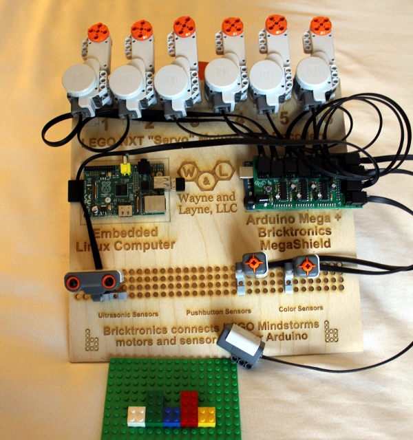
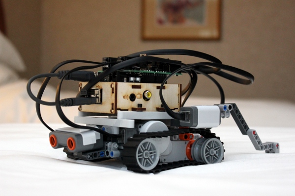
We also created a mobile robot platform, using a LEGO tank platform, an Arduino with Bricktronics Shield, and a Raspberry Pi. Again using the WiFi network connection and a tablet, you can wirelessly drive the tank and read the sensor values.
Once we get more hardware information about the upcoming LEGO Mindstorms EV, we’ll be working on a single-board solution for bringing the power of embedded Linux to LEGO Mindstorms electronics.
For more information about any of these cool projects, subscribe to our RSS feed, or check back in the future for more info.
Note: Wayne and Layne, LLC and our products are not connected to or endorsed by the LEGO Group. LEGO, Mindstorms, and NXT are trademarks of the LEGO Group.
At Wayne & Layne, we design a lot of circuit boards. During the request-for-quote (RFQ) process for getting a PCB fabricated, the outside dimensions of the PCB are an important driver of the overall per-unit price. As part of the W&L “prepare PCB for RFQ” process, we have a little script that uses the PCB’s board outline Gerber file to determine the dimensions of the PCB’s bounding box.
Pass in the filename of the PCB “board outline” Gerber file, and it will print out the dimensions in both the original units (decimills for Gerbers exported from Kicad) as well as inches (again, assuming decimills). It does this by analyzing all the lines of the gerber file, and determining the minimum and maximum in both x and y directions. The script is based on a little chunk of code written by @laen on Twitter (who makes no claim to the code, and also runs the most excellent OSH Park PCB service). We’re releasing this script into the Public Domain, use it however you like.
#!/usr/bin/env python # Gerber query script # Usage: ./gerber_query.py board_edges.gbr # Written by Matthew Beckler for Wayne and Layne, LLC # Based on a script from @laen # Released into the Public Domain. Have fun def main(): import sys if len(sys.argv) < 2: print "Usage: %s gerberfile" % sys.argv[0] sys.exit() import re filename = sys.argv[1] xmin = None xmax = None ymin = None ymax = None for line in file(filename): results = re.search("^X([\d-]+)Y([\d-]+)", line.strip()) if results: x = int(results.group(1)) y = int(results.group(2)) xmin = min(xmin, x) if xmin else x xmax = max(xmax, x) if xmax else x ymin = min(ymin, y) if ymin else y ymax = max(ymax, y) if ymax else y print "Board dimensions:" w = xmax - xmin h = ymax - ymin w_in = w / 10000.0 h_in = h / 10000.0 w_mm = w_in * 25.4 h_mm = h_in * 25.4 print " (%d, %d) original units" % (w, h) print " (%.4f, %.4f) inches" % (w_in, h_in) print " (%.4f, %.4f) mm" % (w_mm, h_mm) if __name__ == "__main__": main() |
Kicad Tutorial: Gerber file generation
This is part of a series of short tutorials on advanced topics of using Kicad, the favorite schematic/PCB design software here at Wayne and Layne.
Once you’ve finished working on your PCB and are ready to send it off for fabrication, one step remains: “Plotting” the PCB design to Gerber files. The Gerber file format is a very old format with its roots in the 1960s, and is used to completely describe a single layer of a PCB design. You need to generate one gerber file per layer of your PCB design (Copper, SolderMask, and SilkScreen, for both the top and bottom sides, plus the PCB Edges layer). The information about where the holes are drilled, and what size the hole should be, are stored in a separate file with a different format, called the Excellon format, named after the market leader in CNC drilling machines during the 1980s.
To generate the gerber and drill files for production, click on the Plot toolbar button in PCBNEW. It is located in the top toolbar and looks like a printer with a “P” overlaid. This brings up the plot dialog box. (Click to enlarge image.)
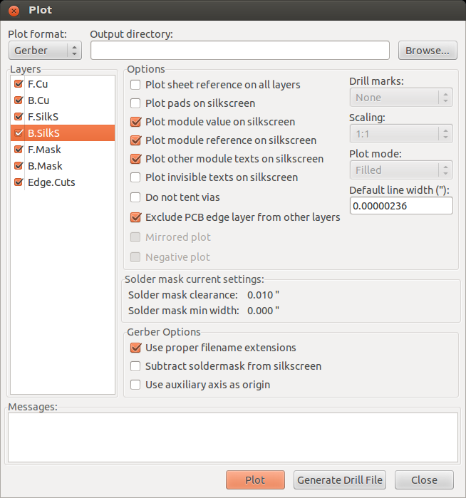
Here, ensure that the “Plot format” is “Gerber”. Leave the “Output directory” field blank, and it will default to saving the files into the project directory. Make sure you check all the layers you want to send to production. If you didn’t use back-side silkscreen, or don’t want to use any back-side silkscreen (some places charge extra for that), you can un-check the B.SilkS layer. The other checkmark boxes are the defaults, but ensure that “Exclude PCB edge layer from other layers” and “Use proper filename extensions” are checked. Press “Plot” to generate the files, one per layer. You will see output in the “Messages:” box at the bottom. When that is finished, click “Generate Drill File” to bring up the next dialog box. (Click to enlarge image.)
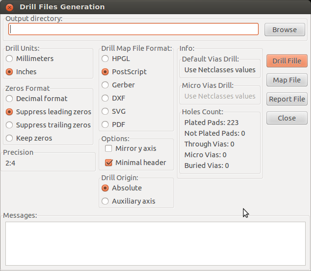
Again, leave the “Output directory” text field empty. The settings here are very important, especially the Drill Units (Inches), Zeros Format (Suppress leading zeros), and Options (Minimal header). You absolutely must check “Minimal header” and un-check “Mirror Y-Axis”. Since we aren’t making a drill map, the “Drill Map File Format” option doesn’t matter. Click the “Drill File” button to generate the drill file. Then press “Close” and “Close”.
Now you can zip up the generated gerber/drill files and send them off for fabrication. At Wayne and Layne, we really like the prototype PCB fabrication services from OSH Park. They describe themselves as
This is a community printed circuit board (PCB) order. We take designs from lots of people, put them all together on a panel and then order the panel from a fab. Since we’re all splitting the panel setup cost, this lets us make circuit boards inexpensively.
This service grew out of the DorkbotPDX PCB Order run by @laen and now comprises of a two-layer panel every other day, a four-layer panel every three weeks and a periodic two-layer medium run service for people needing more than 150 square inches of board.
They have very inexpensive rates, decent production time, and very high-quality output. Plus, the gold and purple boards just look very nice! Here are the details about pricing and design rules (minimum clearance and trace width, minimum hole size, etc).
Other tutorials in this series:
Kicad Tutorial: Using the autorouter
This is part of a series of short tutorials on advanced topics of using Kicad, the favorite schematic/PCB design software here at Wayne and Layne.
Routing, the process of connecting all the pads of a printed circuit board (PCB) layout, can be a time-consuming and tedious process. To avoid the time and frustration of manually routing your PCB, there are various software tools called autorouters which can do this for you. This post will show you how to use the external autorouter from the FreeRouting website.
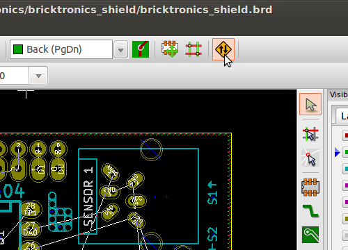
First, ensure that you have selected the proper trace thickness and clearance values in Kicad’s PCBNEW application, by going to “Design Rules”->”Design Rules”. Once you have confirmed the design rule settings, press the “traffic sign” icon in the top toolbar to bring up the FreeRoute interface.
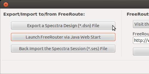
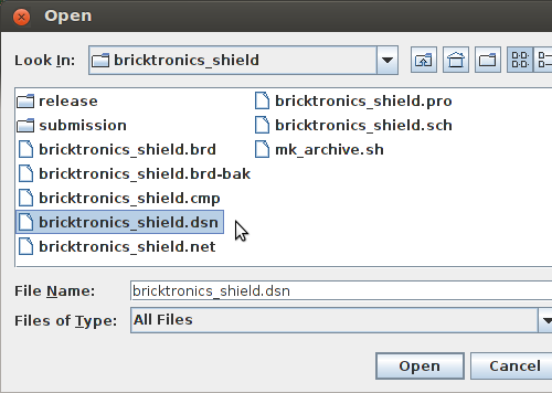
The three buttons on the left will let us export the DSN file that is input to the autorouter, launch the autorouter application, and finally import the SES file that was exported from the autorouter. To start with, press the top button on the left, “Export a Specctra Design (*.dsn) File”. This will open up a file save dialog box, and you can just accept the filename as the default filename is correct.
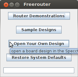
Now, click the second button to launch the autorouter. This utilizes the Java Network Launching Protocol (JNLP), which downloads a small XML file that is used by your Java system to download the rest of the autorouter. You may see a browser window open up briefly when the JNLP file is downloaded. Chrome gives a warning about the file type, you can press “keep” to retain the file for use. Your browser might do the Right Thing with the .jnlp file, and open it with Java. If not, you can probably double-click the downloaded freeroute.jnlp file to launch it, or on Linux you can type “javaws freeroute.jnlp”. When the Freerouter window opens up, click “Open Your Own Design”.
Due to the Java security restrictions, unsigned applets downloaded from the web are not trusted very much, so you have to give it permission to read files on your machine. For whatever reason, on my computer it won’t let me check “Always allow this action”, so it asks me every time.
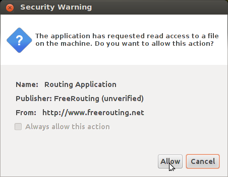
Click “Allow” and then navigate to select the .dsn file you exported from PCBNEW earlier. Click on “Open” and it will load your design.
When your design has finished loading (which may take a minute or two) all you need to do is to click the “Autorouter” button, then sit back and watch the magic happen. The autorouter will do an initial route, then go through a series of optimization steps to try and reduce the number of vias used, as well as trying to reduce the total trace length.
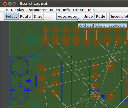
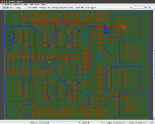
You can wait for the optimization steps to finish, or you can click once in the board area to interrupt the optimization if you are in a hurry, or the results are already good enough.
When you are satisfied with the routing, use the “File”->”Export Specctra Session File” menu option to save the routing results to the .ses file. You will likely get another security warning, click “Allow” to continue. Navigate the file system to where you found the .dsn file, and save as the same filename but with a .ses extension.
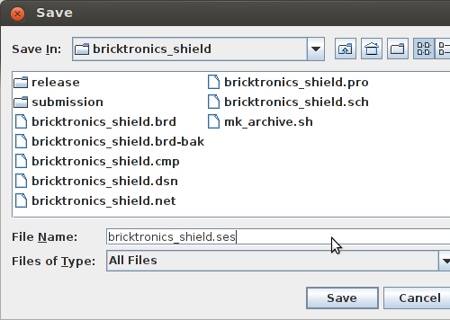
In PCBNEW, select the third and final button on the left. It will open a file select dialog box, and it should already have selected the .ses file you just exported from the autorouter. Accept the filename and Kicad will load the file into your design. It will ask if you want to reload the board connectivity. I’m not exactly sure what this means, but I always click “Yes”.
As a side note, some people dislike autorouters, considering their own manually-routed designs to be superior, and there’s some truth to that feeling. Sometimes the autorouter makes silly decisions, sometimes I can spot ways to route things different and save a via or two, but generally I prefer to let the autorouter have a go at it, then clean up the results.
Other tutorials in this series:
Kicad Tutorial: Copper pours / fills
This is part of a series of short tutorials on advanced topics of using Kicad, the favorite schematic/PCB design software here at Wayne and Layne.
A copper pour or fill refers to an area on a printed circuit board where the original copper is not etched away, and remains in place, usually electrically connected to the Ground signal, producing a “Ground Plane”. This has a number of advantages, including decreasing the amount of etching fluid required during manufacturing, as well as reducing the amount of electrical noise and signal crosstalk experienced by the circuit elements.
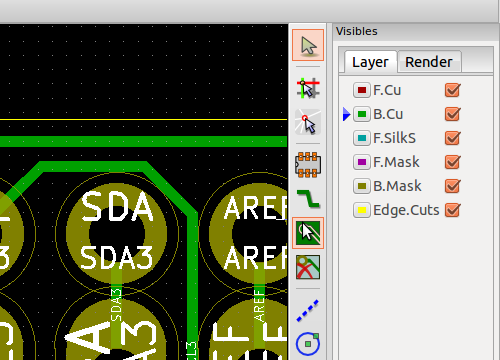
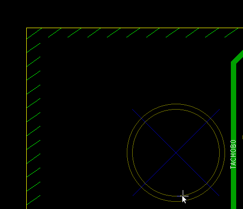
It is relatively easy to create a copper fill in Kicad. We usually add fills after having already drawn in the PCB outline in the Edges layer. First, ensure that you have selected one of the copper layers (such as “Front†or “F.Cuâ€). Then, select the “Add Filled Zones†from the toolbar on the right side of the screen.
Next, click in one corner of the PCB outline to start drawing the copper fill.
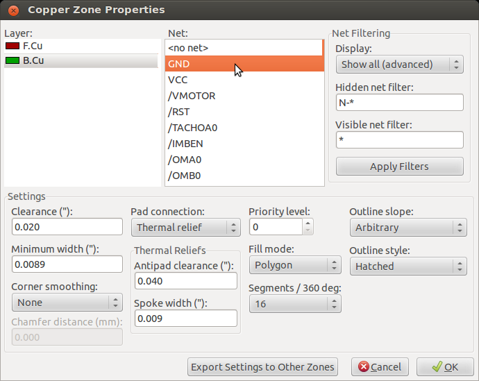
Once you click in the first corner, the following properties box will appear. Select the relevant copper layer (here, either “F.Cu” or “B.Cu”) and the desired net for the fill (usually you want “GND”, but sometimes you might want some other net, or “<no net>” which will make an isolated copper fill). The settings in the bottom half are important for controlling the drawing of the filled area as well as the “thermals”. One potential problem with adding ground fill is that the ground pads will become very difficult to solder, as the ground plane will suck away all the heat from your soldering iron, and the pad won’t ever heat up hot enough for the solder to flow. To avoid this problem, you almost always want to add “thermal relief” to your ground pads, which means there is a keep-out area adjacent to each ground pad where there is no fill, and instead each ground pad is connected by a number of thinner traces. This still provides a very good electrical connection for the ground pad, but makes it much easier to solder. The “Clearance” setting controls the general clearance between the filled area and pads/traces of other nets. The “Minimum width” setting controls the thinnest that the fill can be when flowing around other pads/traces. The “Thermal Reliefs” settings control the clearance around the ground pads (0.040″ here) and the width of the traces connecting from the fill to the ground pads (0.009″ here). We’ve found these settings to work pretty well for most of our projects. You also want to select “Arbitrary” for the “Outline Slope” setting to make it easier to draw the zone outline. Click “OK” to close this window and continue drawing the fill outline. (Click the image to enlarge)
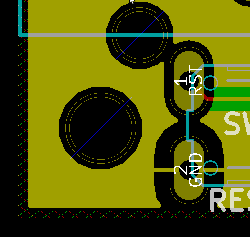
Once you have closed the zone properties window, click once in each of the other three corners (in order) on the board outline. Then, to complete the final segment, double-click on the original corner to end the zone. You should see red or green hatching (depending on which copper layer you used) on the edges of your PCB indicating the filled region, as shown in the image below.
Generally you want to have a copper fill on both the top and bottom of the PCB. To add the fill on the other side, the easiest way is to right-click on the existing board edge, select “Zone outline”, then go to “Zones”->”Duplicate Zone”. This brings up the zone properties box for the new zone, so select the other copper layer and press “OK”.
To see the copper fills in your design, click on the “Show filled areas in zones” button, the 10th button in the left-size toolbar. The button below that will hide the fills. Then, you can run the DRC tool (Ladybug Checkmark in the top toolbar) which will fill all your zones. You should see something like the image below. The brown-yellow color is the combination of red (top side) and green (bottom side) copper fills. We can see the 20 mil clearance between the fill and non-ground copper, and the larger 40 mil clearance between the fill and GND pads.
Other tutorials in this series:
Kicad Tutorial: PCB edges
This is part of a series of short tutorials on advanced topics of using Kicad, the favorite schematic/PCB design software here at Wayne and Layne.
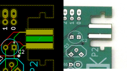
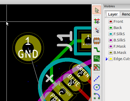
An important part of designing a PCB is to clearly indicate the outline of the board, so the board house will know how to cut your boards apart. Most PCBs are rectangular, but sometimes you want to add a more complex outline (like a circle or hexagon) or a very complex outline (like the PCB for the Video Game Shield, shown below).
To make it easier to determine where the PCB edges should be, you probably watch to switch your cursor to be the full-screen cross, by clicking the cursor toggle button in the left-most toolbar (6th down from the top).
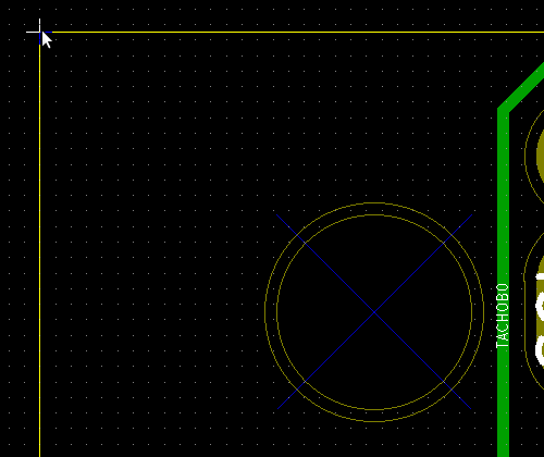
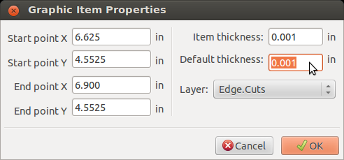
Then, select the “Edge.Cuts” layer from the list on the right side of the screen. Select the blue dashed line toolbar icon to draw graphic lines in the Edge.Cuts layer. Using the full-screen cross cursor, it is easy to find the corner of your design. Make sure to leave a little bit of clearance between the outer-most components and the PCB edge. Click to start drawing the edges, and click once in each corner of the PCB. Double-click to end the drawing.
If your edge lines are not very thin, we suggest reducing their width. Right-click on each line (you might have to zoom in to ensure that your mouse cursor is pointing at the yellow line itself) and select “Edit Drawing”. Then, change the Item and Default thickness values to be 0.001″ each. We feel that this reduces confusion with the board house as to where exactly the board should be cut (“Inside of the thick line? Outside of the thick line? Middle of the thick line?” With a thin line there is no ambiguity.)
Other tutorials in this series:
W&L were mentioned in this interview with Ladyada, conducted by Brad Hines:
BH: Name what you would say are the biggest devices behind the DIY movement.
…
Open-source hardware, this is more general, but there are many companies, from Adafruit to Sparkfun that have release hundreds of open-source hardware products. From breakout boards to watch kits – we’re all putting value back in while we do a great job getting our customers and communities awesome products. We really like Evil Mad Scientist, LittleBits, Wayne and Layne, Seeed, Bunnie studios and many many more who have devoted their passions to sharing hardware.
Wayne & Layne Forum: Down for the count
The W&L forum is basically non-functional right now after an issue at our webhost, and we’ll be re-installing and re-configuring the forum in the next few days. We expect it’ll be back up before Monday, and we’ll post here when it’s ready. Sorry for the the confusion and non-functionality the last few weeks!
Solderbot makes and sells assembled electronics kits. They’re relatively new, and look to be stocking at least one kit from each of the the Minneapolis kit companies I know about!
They’ve got our Blinky Grid and Blinky POV for sale, and the video Luke made is a pretty great introduction to the kit!
New store!
Last night, we opened our new webstore at https://store.wayneandlayne.com. We’re keeping the old one up until the end of the holidays, but the new one has the same prices, and works much better!(We’ve since added redirects for the pages, products, and categories, so you shouldn’t be able to get to the old site.)
In fact, you can find the Bricktronics Shield in the new store.
More announcements coming soon!